Old PCB info.
For newest PCB go to HERE!
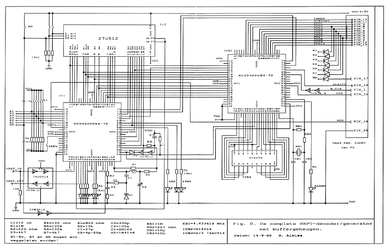
Postscript file schema.
Note: The part around the RAM in this schema and the colored looks a bit different, but is
in essence the same. This file (300k) gives al details.
In the small (colored) one (33k) text is not very clear.
Postscript gives perfect picture, if you have tools to handle it.
Print lay-out decoder.
Pushing FPGA's into their sockets sometimes needs some force. Removing them without damaging them or the sockets can be difficult without proper tools.
Make sure that you push the FPGA's in the right way into their sockets.
But first read Put into use.
The print contains a few jumpers (connections) called J1-J6.
Only J1, J3 and J6 have to be added.
J2, J4 and J5 (instead of J6) are for an old mode, which uses 3 steps to transport the 12 bits to the computer. This is only needed if the parallel port
can not be used as a bidirectional port.
J1 is switch HSEL in the schematic, remove if you want to select channels by means of switches instead of via the software. It is highly recommended to use the software to select channels, because this information is also saved in the data file, togeher with the picture.
S1 and S2 select 1 of 4 segments of the EPROM:
- S1=SD in the schematic: select HRPT/PDUS
- S2=SX in the schematic:
- 512k EPROM: OFF (selects second half of EPROM, which is normally empty).
- 256k EPROM: ON (pin 1 of this type should be +5V).
Suggestion: Use a real switch for S1, and a wire (or no wire) for S2 (or use a DIP-switch for this one).
Note: Unfortunately, numbering of a few components in the schematics don't match with the parts shown in the PCB. These are:
| schema | print | value | comment
|
| R8 | R10 | 10k |
|
| RS (6x) | R8 | 10k (6x array) |
|
| R9 | R11 | 1M |
|
| R10 | R12 | 220 ohm |
|
| RS (3x) | R13,R14,R15 | 10k |
|
| C5 | C6 | 10p |
|
| C6 | C7 | 10p |
|
| C7 | C5 | 10u |
|
| C8 | C8 | 100n |
|
| --- | C9 | 100n | (extra C on PCB)
|
| diodes near K1-KM | D3-9 | 7x1n4148 |
|
Furthermore, A13 of the EPROM is connected to KM in the schema but on the PCB it is connected after the 2 inverters IC6. This is done to make lay-out easier, but has no functional consequences.
The print is designed by W. Pfeifer. The GIF-pictures are here to get an idea of the print layout. Resolution is, however, far too low to use it as a masker.
Use the postscript file instead.
Postscript file PCB copper side.
NOTE: Scale is 1:1.414. Reduce 71% (A3 ==> A4). Picture is in reverse!
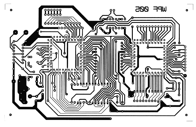
PCB component side.
