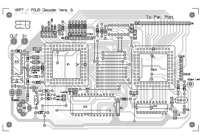
Schematic and PCB of the decoder/generator.
| Schema decoder PDF | Print PDF |
|---|---|
|
|
|
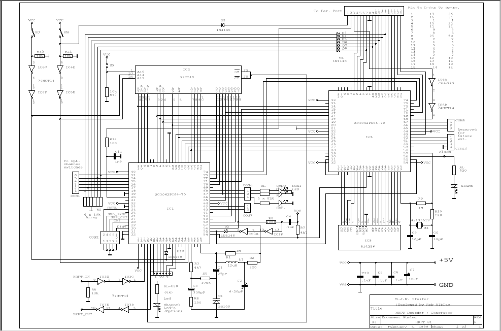
Six optional channel switches may be connected to CON1 (between CON1 and +5V), to select one or more of the 5 HRPT-channels and/or the remaining info present in the HRPT-frame.
Normally, you don't need these switches because selection is done by means of the computer, via the parallel port. If you want to use the switches, then remove D3-D8 and remove the connection on CON2 between pin 1 and 2. (Note that the correct info which channels are selected is saved in the file! Selecting different channels via hardware and software could give corrupt files!)
Selecting channels at the hardware instead of by means of software has the advantage that the data rate to the computer is lower, so a slow computer can be used to record e.g. 1 channel.
The data selector is not suitable for Seawifs; in this case all channels have to be recorded.
In PDUS mode channel selection is not possible.
The 2 switches and jumper at the top select a segment of the EPROM. For the current EPROM the meaning is:
| SD | SX | SM | |
|---|---|---|---|
| HRPT decoder | open | open | open |
| HRPT generator | open | open | closed |
| HRI decoder | closed | open | open |
| HRI generator | closed | open | closed |
| CHRPT decoder | closed | closed | open |
| CHRPT generator | closed | closed | closed |
| (HRPT decoder copy) | open | closed | open |
| (HRPT generator copy) | open | closed | closed |
Just selecting another segment of the EPROM is not sufficient; the FPGA has to load the new selected content. This is done by means of the components connected to pin 55. It works only for switching between HRPT/PDUS/decoder/generator. If jumper SX is closed or opened the power has to be disconnected for a short while, to force a reload. (You can also connect pin 55 to GND for a short while.)
At the bottom of IC1 there are 6 LEDS, showing which channels are selected.
The components around inductor L1 determine the central frequency of the VCO of the PLL; R3, R4 and C3 act as loop filter. Pin 50 is the output of the phase comparator (EXOR type).
More to the right a LED 'err' shows if there are data errors and/or PLL lock problems. The dual-LED shows if the decoder is in-sync:
On connector block CON2 pin 1 has to be connected to pin 2; the remanining pins should be unconnected. See the data sheets for description of the pins connceted to it.
On connector block CON7 you can add LEDs for separate PLL (1) and data (2) error indication, if you like. LED ERR on CON 6 is a ORed version of these 2 pins.
IC5 is a 256kx4 bits dynamic RAM; IC4 (the second FPGA) acts as RAM controller. The buffer is able to handle 64k words of 12 bits each.
The frequency of the XTAL is not very important; a suitable value is 4.43 MHz (TV PAL XTAL); but any value between 1 and 5 MHz should work.
At the right-top the connection with the parallel port of the PC is shown. Note that a part is used bidirectional (input: selection of channels; output: 6 of the data bits). Best is to use a parallel port of type EPP, but an old fashioned type with open-collector output is also OK.
The 12 data bits going to the PC are:
See conflict warning!