Schema decoderPrint

Schema decoder |
|
|
|---|
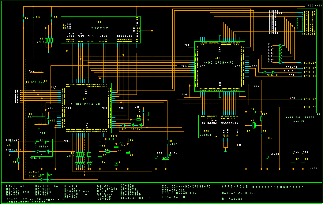
Switches S1-S5 are there to select one or more of the 5 HRPT-channels; SI selects the remaining info present in the HRPT-frame. These switches are not really needed, because selection is possible (and recommended) by means of the computer, via connections K1-KI.
Selecting channels at the hardware instead of by means of software has the advantage that the data rate to the computer is lower, so a slow computer can be used to record e.g. 1 channel.
The data selector is not suitable for Seawifs; in this case all channels have to be recorded.
In PDUS mode channel selection is not possible.
The 3 switches at the top select a segment of the EPROM. SM selects either decoder or generator; SD selects HRPT or PDUS. SX selects the upper half of the EPROM; it is not needed, except if a second version of the decoder/generator should be available. In that case, a 512k EPROM is needed.
Note that switch SM is not needed because selection of decoder/generator is possible by means of the computer (connection KM). SD is needed; all parallel port registers are in use so selection via computer is not possible.
Just selecting another segment of the EPROM is not sufficient; the FPGA has to load the new selected content. This can be done by switching off the power for a short while, or by making pin 55 of the FPGA low. The components connected to this pin are there to do an automatic reload as soon as a new segment (switches SM or SD) is choosen.
At the bottom of IC1 there are 6 LEDS, showing which chammels are selected.
The components around inductor L1 determine the central frequency of the VCO of the PLL; R3, R4 and C3 act as loop filter.
More to the right a LED 'err' shows if there are data errors and/or PLL lock problems. The dual-LED shows if the decoder is in-sync:
IC5 is a 256kx4 bits dynamic RAM; IC4 (the second FPGA) acts as RAM controller. The buffer is able to handle 64k words of 12 bits each.
The frequency of the XTAL is not very important; a suitable value is 4.43 MHz (TV PAL XTAL); but any value between 1 and 5 MHz should work.
At the very right the connection with the parallel port of the PC is shown. Note that a part is used bidirectional (selection of channels / 6 of the data bits). Best is to use a parallel port of type EPP, but an old fashioned type with open-collector output is also OK.
The 12 data bits going to the PC are: 10 data bits, in-sync info and start-of-frame info.